Project 2: Deterministic integration of wavelength-tunable single-photon sources with waveguides and detectors in a III-V platform
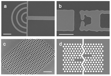
InAs QDs have the best optical properties of any known Quantum Emitter, but they are challenging to integrate into photonic devices for two reasons. First, typical MBE-grown InAs QDs are randomly distributed across the growth surface, which makes it impossible to deterministically align photonic devices to more than one QD. Second, each QD emits photons with slightly-different photon wavelengths, which makes it impossible to deterministically match the QD photon wavelength to the design wavelength of photonic devices. This project takes advantage of two recent advances to overcome these challenges. First, Zide has demonstrated successful deterministic placement of single QDs with an occupancy of 90% in 10 µm spaced nano-holes patterned into the substrate, a significantly lower density of patterned QDs than has previously been shown in literature. [Reference] This low density is critical for integration with photonic crystal cavities or other optical elements such as those shown in Fig D.Second, the optical elements we will use are a pair of closely-spaced QDs. As illustrated in Fig. E, the emission energy of an “indirect exciton” in such a QD pair can be tuned strongly with applied electric field because the electron and hole are located in separate QDs. Coherent tunneling between the two QDs that comprise the pair also leads to unique “molecular” features. These features provide powerful new functionality for quantum device applications. [ Ref 1, Ref 2 ]
The goals of this project are to: a) study the quality of the quantum emitters as a function of the growth conditions (Zide / Doty), b) integrate the strain-templated growth into the structures required to fabricate photonic components such as those shown in Fig. D (Zide), c) realize new photonic device components (e.g. Fig. Ed) that enable application of different electric fields to each QD pair (Doty), and integrate these QDs into photonic waveguides that terminate in traveling wave Superconducting Nanowire Single Photon Detectors (see Fig. F) (Osinski) to enable fully-on-chip quantum measurements.

Fig E Caption: QDM photoluminescence as a function of applied electric field. Insets: schematic band diagrams of states of a QDM in which holes tunnel between the two QDs. Wavelength-tunable indirect exciton emission is highlighted

